


US9379321
[0023] In some embodiments, the package substrate 421 may be an epoxy-based laminate substrate having a core and/or build-up layers such as, for example, an Ajinomoto Build-up Film (ABF) substrate.
【0016】
いくつかの実施形態において、パッケージ基板421は、例えば、味の素ビルドアップフィルム(ABF)基板などの、コアおよび/またはビルドアップ層を有するエポキシベースの積層基板であり得る。

The package substrate 421 may include other suitable types of substrates in other embodiments including, for example, substrates formed from glass, ceramic, or semiconductor materials.
パッケージ基板421は、例えば、ガラス、セラミック、または半導体材料から形成された基板などの、他の適切な複数のタイプの基板を他の複数の実施形態において含み得る。
[0024] The package substrate 421 may include electrical routing features configured to route electrical signals to or from the die 402 .
【0017】
パッケージ基板421は、ダイ402への、またはダイ402からの電気信号をルーティングするよう構成された電気ルーティング構造を含み得る。
The electrical routing features may include, for example,
電気ルーティング構造は、例えば、
package contacts (e.g., pads 410 ) disposed on one or more surfaces of the package substrate 421 and/or
パッケージ基板421の1つまたは複数の表面に配置されたパッケージ接触部(例えば、パッド410)、および/または、
internal routing features (not shown) such as, for example, trenches, vias or other interconnect structures to route electrical signals through the package substrate 421 .
例えば、トレンチ、ビア、または、パッケージ基板421を介して電気信号をルーティングする他の相互接続構造などの、内部ルーティング構造(不図示)を含み得る。
US11200385
[0068] As shown in FIG. 2, the electronic card 200 includes a laminated substrate that includes a first layer 201 and a second layer 203 .
【0068】
図2に示すように、電子カード200は、第1の層201及び第2の層203を含む積層基板を含む。

[0075] The substrate 302 a , in this example and with regard to other examples described herein, may be formed from a single material or may be formed from multiple materials that are bonded or laminated together.
【0075】
基板302aは、本例及び本明細書で説明する他の例に関して、単一の材料から形成されてもよく、又は互いに結合又は積層される複数の材料から形成され得る。
For example, the substrate 302 a may be formed from a metal material (e.g., a metal sheet) including, for example, aluminum, carbon steel, stainless steel, titanium, or other type of metal or metal alloy.
例えば、基板302aは、アルミニウム、炭素鋼、ステンレス鋼、チタン、又は他の種類の金属又は合金を含む金属材料(例えば、金属シート)から形成され得る。
The substrate 302 a may also be formed from one or more polymers (e.g., a polymer sheet or film) including, for example, polyvinyl chloride, polyethylene-based polymers, PVC, polyester, acrylic, styrene, or(例の列挙なのだから、andの方が良さそうに思える)polycarbonate.
基板302aはまた、例えば、ポリ塩化ビニル、ポリエチレン系ポリマー、PVC、ポリエステル、アクリル、スチレン、又はポリカーボネートを含む1つ以上のポリマー(例えば、ポリマーシート又は膜)から形成され得る。
In some implementations, the substrate 302 a is formed from a composite material, which may include a filled polymer, carbon fiber, carbon laminate, or other structure formed from two or more materials.
いくつかの実施例では、基板302aは、充填ポリマー、炭素繊維、炭素積層体、又は2つ以上の材料から形成される他の構造を含み得る複合材料から形成される。
In some cases, the substrate 302 a may be formed from a ceramic, glass, or other similar type of material.
場合によっては、基板302aは、セラミック、ガラス、又は他の同様の種類の材料から形成され得る。
The substrate 302 a may be formed as a unitary or homogenous element or, alternatively, may be formed from a laminate of multiple materials or multiple layers (e.g., multiple sheets and/or films) that are bonded or adhered together.
基板302aは、単一要素又は均質要素として形成され得る、あるいは、互いに接合又は接着される複数の材料又は複数の層(例えば、複数のシート及び/又は膜)の積層体から形成され得る。
For example, the substrate 302 a may be formed from a metal sheet (e.g., titanium sheet) and bonded or laminated to one or more polymer sheets (e.g., plastic sheets) to form a laminated multi-layer substrate.
例えば、基板302aは、金属シート(例えば、チタンシート)から形成され、1つ以上のポリマーシート(例えば、プラスチックシート)に結合又は積層されて、積層多層基板を形成し得る。
In one example, the substrate 302 a includes a metal sheet that is bonded to two plastic sheets, each plastic sheet bonded to opposite surfaces of the metal sheet.
一例では、基板302aは、2枚のプラスチックシートに結合された金属シートを含み、各プラスチックシートは、金属シートの対向面に結合されている。
In another example, the substrate 302 a includes a single plastic sheet that is bonded to a surface of the metal sheet.
別の例では、基板302aは、金属シートの表面に結合される単一のプラスチックシートを含む。
An adhesive or other bonding agent may be used to bond multiple layers together.
接着剤又はその他の結合剤を使用して、複数の層を結合し得る。
As shown in FIG. 8B, each of the first conductive layer of terminal electrodes 819 b , 821 b , 829 b is electrically coupled to the rear conductive layer 831 b by a corresponding via, 822 b , 824 b , 826 b , that extend through the plate substrate 810 b .
図8Bに示すように、端子電極819b、821b、829bの第1の導電層はそれぞれ、プレート基板810bを貫通する対応するビア822b、824b、826bによって背面導電層831bに電気的に接続される。

The vias 822 b , 824 b , 826 b may be formed by drilling holes through the plate substrate 810 b and then filling the holes with a conductive material.
ビア822b、824b、826bは、プレート基板810bに穴を開け、次にその穴に導電材料を充填することにより形成され得る。
In some cases, the vias 822 b , 824 b , 826 b are formed when forming the rear conductive layer 831 b .
場合によっては、ビア822b、824b、826bは、背面導電層831bを形成するときに形成される。
The vias 822 b , 824 b , 826 b and the rear conductive layer 831 b may be formed from the same conductive material.
ビア822b、824b、826b及び背面導電層831bは、同じ導電材料から形成され得る。
US2019189327
[0026] FIG. 2A shows a perspective view of a vertical inductor structure 210 according to aspects of the present disclosure.
【0014】
図2Aは、本開示の態様による垂直インダクタ構造210の斜視図を示す。
FIGS. 2B-2D show end and cross-sectional views of the vertical inductor structure 210 embedded in laminate stacked(*ラミネート(基板)を積層した)substrates.
図2B~図2Dは、ラミネート積層基板に埋め込まれた垂直インダクタ構造210の端面図および断面図を示す。
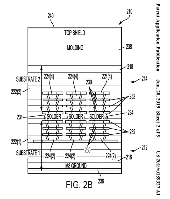
The vertical inductor structure 210 may include a first portion 212 and a second portion 214 .
垂直インダクタ構造210は、第1の部分212と第2の部分214とを含んでもよい。
The first portion 212 of the vertical inductor structure 210 may be formed in a first laminate substrate 216 , and the second portion 214 may be formed in a second laminate substrate 218 .
垂直インダクタ構造210の第1の部分212は、第1のラミネート基板216内に形成されてもよく、第2の部分214は、第2のラミネート基板218内に形成されてもよい。
Each of the first laminate substrate 216 and the second laminate substrate 218 may have any number of a plurality of layers, for example, between 2 layers and 10 layers.
第1のラミネート基板216および第2のラミネート基板218の各々は、任意の数の複数の層、たとえば、2層から10層の間の数の層を有してもよい。
US10826147
[0002] Radio frequency (RF) and electromagnetic circuits may be manufactured using conventional printed circuit board (PCB) processes.
【0002】
無線周波数及び電磁回路は、従来のプリント回路基板プロセスを用いて製造することができる。
Conventional PCB manufacturing processes may include lamination, electroplating, masking, etching, and other complex process steps,
従来のPCB製造プロセスは、積層、電気メッキ、マスキング、エッチングその他の複雑なプロセスステップを含むことがある。
and may require multiple steps, expensive and/or hazardous materials, multiple iterations, extensive labor, etc.,
また、複数のステップ、高価な及び/又は危険な材料、複数回の反復、大規模な労力などを必要とすることがあり、
all leading to higher cost(*無冠詞;具体的な数値が問題ではない)and slower turnaround time.
これら全てによって、コストが高くなり、ターンアラウンド時間が遅くなる。
Additionally, conventional PCB manufacturing processes have limited ability to allow for small feature sizes, such as transmission line (e.g., stripline) dimensions, and dimensions of dielectric materials between conductors (e.g., dielectric thickness, inter-via spacing, etc.),
さらに、従来のPCB製造プロセスは、伝送線路(例えば、ストリップ線路)の寸法、及び導体間の誘電体材料の寸法(例えば、誘電体の厚さ、ビア間の間隔など)のような小さな特徴サイズを可能にする能力が限られており、
thereby limiting the range of highest frequency signals that may be supported by such circuits.
それによって、そのような回路によって支持され得る最高周波数信号の範囲が制限される。
[0003] Aspects and embodiments described herein provide simplified circuit structures, and manufacturing methods thereof, for conveyance of electrical signals, especially radio frequency signals, within a circuit.
【0003】
本明細書に記載される態様及び実施形態は、回路内で電気信号、特に無線周波数信号を伝達するための簡略化された回路構造体及びその製造方法を提供する。
Various embodiments of circuits in accordance with those described herein may be constructed of, e.g., laminate or dielectric substrates, and may have circuit features, signal layers, ground planes, or other circuit structures therebetween.
本明細書の記載に従った回路の様々な実施形態は、例えば、積層基板又は誘電体基板から構成されてもよく、回路特徴、信号層、接地平面、又はそれらの間の他の回路構造体を有してもよい。
US2021028346
Stacking the partitioned substrate sheets may entail introducing an adhesive between the substrate that is cured so that the stacked substrates are bonded together.
分割された基板シートを積み重ねることは、積層基板が一緒に接合されるように、硬化した基板の間に接着剤を導入することを伴う場合がある。
Alternatively, the partitioned substrate sheets may be bonded together using adhesiveless bonding techniques. After obtaining the stacked flexible wiring, further processing may be performed if necessary.
あるいは、無接着結合技法を使用して、分割された基板シートが一緒に接合され得る。積層フレキシブル配線を取得した後、必要に応じてさらなる処理が実行され得る。
For example, additional via contacts may be formed within one or more of the stacked substrates to provide connections to conductive traces on the stacked flexible wiring.
たとえば、積層フレキシブル配線上の導電性トレースへの接続を提供するために、追加のビアコンタクトが積層基板のうちの1つまたは複数内に形成され得る。


※コメント投稿者のブログIDはブログ作成者のみに通知されます